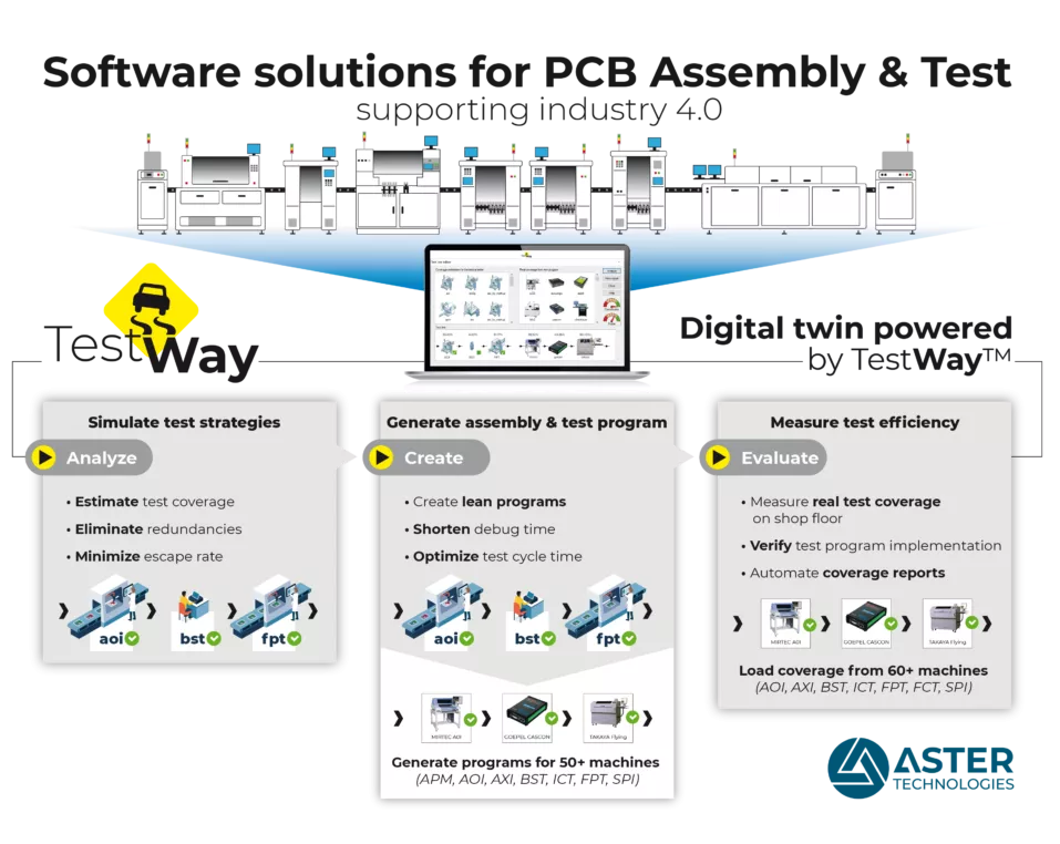
Test coverage analysis software
TestWay Express operates from native CAD formats and is powered by QuadView visualization.
Electrical rules checking enables the identification and rectification of electrical rules violations, before finalizing the board layout.
Probe analyzer automates probe placement with a comprehensive set of rules to define priorities, clearances and constraints and generate detailed accessibility reports.
The software simulates test strategies using test machine models to maximize test coverage and optimize test programs to minimize redundancy between strategies.
The theoretical models estimate the test coverage of each individual stage (SPI, AOI, X-Ray, Boundary scan [BST], In-circuit [ICT], Flying probe [FPT] and Functional test) and optimize the combined results.
TestWay Express generates the output files, aligned on the simulation results, for programming the assembly, test and inspection machines.
By importing the post-debug test programs, test engineers can measure the actual coverage and compare this against the early estimation, to identify gaps in the overall strategy.
twSystem is an add-on module to extend the PCBA viewing and analysis at system level.

D. Billard
Test Expert at Comfort and Driving Assistance System
They trust us to deliver the best value for their software investment


TestWay Express Software Packages

Electrical Rules Checking
Electrical rules checking (eDfT) enables the identification and rectification of electrical rules violations before finalizing the board layout, in order to prevent costly design re-spins.
These rules are distributed into 3 categories: Design rules, Testability rules, Boundary-scan rules. These rules are derived from formal standards and include rules commonly applied throughout the electronics industry.
Specific customer requirements can be specified in a low-code language using the custom rules feature.
- Design rules to verify conformance restrictions imposed by certain technologies, for example; open-collector, bushold, specific termination requirements, noise immunity, etc.
- In-Circuit test rules for insuring test partitioning and initialization pin control, examples; chip select, output enable, test pins, etc.
- Boundary-scan rules for verifying chain integrity, boundary-scan compliance, presence of bypass resistors, flash programming optimization, identifying boundary-scan clusters and boundary-scan bus terminations, etc.
- Custom rules to meet any specific in-house testability requirements
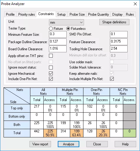
Place the probes
Probes are placed by considering the mechanical (mDfT) and design-for-test (DfT) constraints practiced by respective companies.
Once the possible probe positions have been analyzed, the nail allocation algorithm selects the best of these opportunities for the nail positioning according to the preferences set by the user.
This allows the estimated coverage to be calculated according to the achievable test access.
- Accessibility report is created to provide a list of the nodes that do not have access
- List of probes/nails in Excel format
- Nail retro-annotation back to the schematic
- Generation of customizable DXF and Excellon files
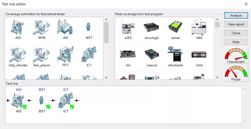
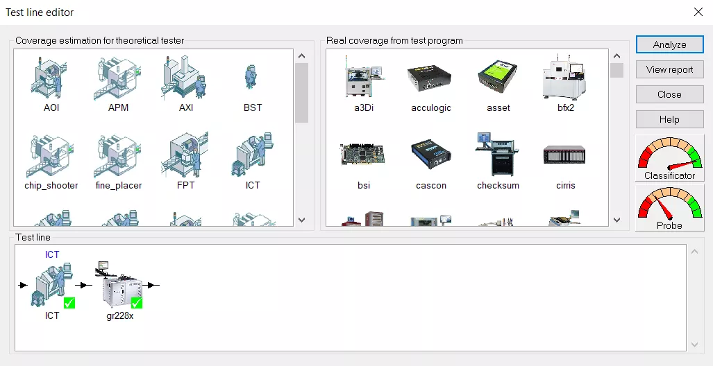
Select manufacturing strategy
When deciding on the optimal test flow, it is important to consider all available test and inspection machines such as AOI, X-Ray, BST, ICT, FPT and Functional test.
The “test line” is easily defined using a simple drag and drop operation.
The theoretical test models, for coverage estimation and the actual test models, for coverage measurement, can be combined to reflect your manufacturing strategy.
Test coverage estimation
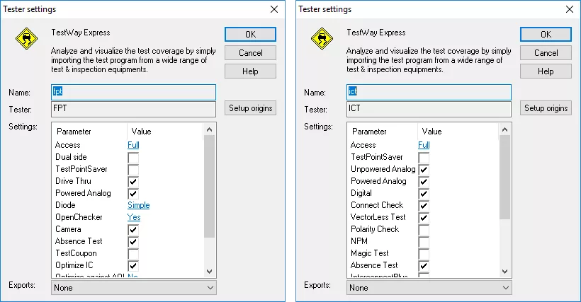
Each of the theoretical test strategies allows selection of tester settings, from a feature list for a particular test strategy.
In order to provide a more accurate estimation, any specific test features that are available on the target tester should be included in the analysis. This aligns the estimated coverage to the real tester coverage.
TestWay Express handles cross optimization along the test line, such as Boundary-Scan or AOI, that can be used to minimize the In-Circuit Test or Flying Probe Test.
Design to build, Design to test
The test strategies simulation results are used to automate the program generation for SPI, Pick-&-Place, Chip shooter, AOI, X-Ray, Boundary-scan, Flying Probe, and In-circuit Test.
Output processors are available for all brands of equipment

In addition to creating the test machine input files, TestWay Express also generates test models for analog multi-element components and digital models, including disable configurations.
Test for Excellence: Check real coverage
The real test coverage is determined after the test has been developed and debugged, by analyzing the test program or coverage reports, from any test and inspection systems.
By analyzing the true coverage, test coverage analysis reports can be created to reflect what is actually being tested.
The coverage analysis is based on industry standard metrics such as:
- PPVS (Presence, Polarity, Value, Solder)
- PCOLA/SOQ (Placement, Correct, Orientation, Live, Alignment / Short, Open, Quality)
By obtaining a reference point from early coverage estimation and comparing this with the coverage provided by the real test program, it is possible to identify deviations in order to drive continuous improvements.
Download Product Brief and White Papers

Why ASTER Technologies ?
We offer comprehensive software tools to simulate a PCBA and the manufacturing/test machines in a digital environment. Digital twin technology allows our customers to ensure PCBA fabrication and improve test coverage, to limit the risk of undetected defects, thereby reducing field failures and costly recalls.