DfT Analysis
Design-for-Test (DfT) is a methodology that involves designing electronic products with testing in mind from the very beginning.
When applied to Printed Circuit Board Assembly (PCBA), DfT ensures that the board is optimized for efficient and comprehensive testing during the manufacturing stage.
This process can be categorized into three distinct types of analysis:
- Electrical rules checking (eDfT) to identify and rectify violations pre-layout
- Test point analysis (DfT) to identify test point requirements from schematic capture
- Mechanical board analysis (mDfT) to place test probes and confirm net access is not compromised by solder mask etc.

By combining eDfT, DfT, and mDfT analyses, ASTER 's solutions enable manufacturers to identify defects, faults and vulnerabilities at an early stage, thereby minimizing costly delays and rework.
Electrical rules checking (eDfT)
ASTER's DfT Checker solution enables the identification and rectification of electrical rules violations before finalizing the board layout in order to prevent costly design re-spins.
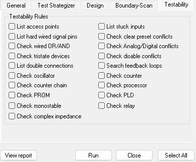
DfT Checker encompasses standard checks pertaining to design, boundary-scan, and testability rules, as well as customer’s specific checks, relating to company requirements.
- Design rules to verify conformance restrictions imposed by certain technologies, for example; open-drain, noise immunity, etc.
- Boundary-scan rules to verify chain integrity, compliance, presence of bypass resistors, flash programming optimization, identifying clusters and bus terminations, etc.
- Testability violations to insure initialization and test partitioning, examples; chip select, output enable, test pins, etc.
Test points analysis (DfT)
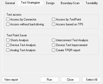
ASTER's TestPointSaver solution facilitates the identification of test point requirements during the schematic capture.
This reduces the need for unnecessary test access, saving on PCB real estate, particularly on high density boards. TestPointSaver features a number of pre-defined algorithms to:
- Identify critical test points to ensure high coverage in case of poor net accessibility
- Optimize the quantity of test points to reduce fixture costs
- Propose alternative locations to balance coverage and cost constraints
Mechanical board analysis (mDfT)
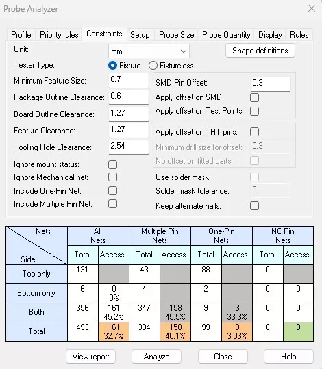
Once the PCBA layout is completed, Probe Placement is carried out, where test probes are precisely positioned to access critical test points.
Additionally, a mechanical DfT analysis must be conducted to confirm the nets that require test access are not compromised by solder mask, component outline, adjacent probes constraints, etc.
ASTER's Probe Analyzer solution allows users to place probes for both fixture and fixture-less systems. It incorporates innovative algorithms to:
- Automate probe placement based on design and test parameters
- Check clearances to confirm test access is not compromised by mechanical constraints
- Specify nets which do not require test access
- Simulate virtual probes to optimize arrangement for maximizing coverage